Classification of metals, insulators and semiconductors
NCERT Class 12 Physics Chapter 14 Sections 14.1–14.2
Quick answer
Metals have partly filled or overlapping bands; insulators have very few thermal carriers at ordinary temperatures, while semiconductor carrier populations can be controlled by doping or excitation. NCERT’s 3 eV boundary is only a rough guide, with silicon about 1.1 eV, germanium 0.7 eV and diamond 5.4 eV. The band gap is Eg = EC − EV.
With your textbook
NCERT Physics Part II (Class 12), Chapter 14 “Semiconductor Electronics: Materials, Devices and Simple Circuits”, Sections 14.1–14.2 “Introduction” and “Classification of Metals, Conductors and Semiconductors”, pages 323–327.
Open the official NCERT chapter (PDF, 1.9 MB, ncert.nic.in) (opens in a new tab)
Checked against the 2025-26 reprint on .
What are metals, insulators and semiconductors?
Metals, insulators and semiconductors
Solids are sorted into metals, semiconductors and insulators by how well they conduct electricity, and the reason lies in their energy bands. In a solid, neighbouring atomic orbitals interact, splitting their allowed energies into many closely spaced levels that form bands. In NCERT’s words:
These different energy levels with continuous energy variation form what are called energy bands.
NCERT Physics Part II (Class 12), Section 14.2, page 325
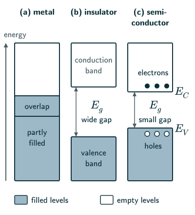
A metal has a partly filled band or overlapping bands. In NCERT’s introductory classification, insulators have a wide gap and semiconductors a smaller gap, allowing appreciable thermal carriers at room temperature (pages 325–327). The 3 eV dividing line is only a rough guide: wide-gap semiconductors also exist.
In plain words: in a solid, electrons can only have energies inside certain bands. If the top band with electrons in it is only partly full, electrons move easily and the solid is a metal. If it is full and the next band is far above, ordinary thermal excitation creates very few mobile carriers: an insulator. If the next band is just a little way up, heat lifts a few electrons across, and the solid conducts a little: a semiconductor.
Classification by conductivity
-
By the relative values of electrical conductivity σ, or resistivity ρ = 1/σ, solids are broadly classified as follows (NCERT page 324):
- Metals: ρ ~ 10−2 to 10−8 Ω m, σ ~ 102 to 108 S m−1;
- Semiconductors: ρ ~ 10−5 to 106 Ω m, σ ~ 105 to 10−6 S m−1;
- Insulators: ρ ~ 1011 to 1019 Ω m, σ ~ 10−11 to 10−19 S m−1.
-
These values only indicate orders of magnitude, and real materials can fall outside them. Resistivity is not the only difference between the three kinds of solid (NCERT page 324).
-
NCERT Chapter 3 gives metals 10−8 to 10−6 Ω m (page 90). The upper end printed here, 10−2 Ω m, is well above that and overlaps the semiconductor range, which starts at 10−5 Ω m: read these ranges only as rough orders of magnitude.
-
NCERT slip (page 340): NCERT Summary point 3 gives insulators a resistivity of more than 108 in ohm per metre. Resistivity is measured in Ω m, and the text on page 324 gives insulators 1011 to 1019 Ω m.
-
Semiconductors may be elemental, silicon (Si) and germanium (Ge), or compound: inorganic, such as CdS, GaAs, CdSe and InP; organic, such as anthracene and doped phthalocyanines; or organic polymers, such as polypyrrole, polyaniline and polythiophene (NCERT page 324).
-
Most devices today use Si, Ge or inorganic compound semiconductors. Devices using organic semiconductors and polymers have been developed since 1990. The chapter deals with inorganic semiconductors, mainly Si and Ge (NCERT pages 324–325).
-
Why semiconductors replaced vacuum tubes: in a vacuum tube, electrons from a heated cathode, by thermionic emission, flow through a vacuum, and the tube is bulky, uses much power, works at high voltages (about 100 V) and has a limited life and low reliability. In a semiconductor device the charge carriers are supplied and flow within the solid itself, with no heating or vacuum, so it is small, uses little power, works at low voltages and has a long life and high reliability (NCERT pages 323–324).
Valence and conduction bands
- In an isolated atom, electrons occupy discrete quantum energy states; Bohr orbits are a useful introductory picture, not the general description of multi-electron atoms. In a solid the atoms are close, so the outer orbits of neighbouring atoms come very close or overlap. Each atomic level then splits into a huge number of closely spaced levels, which form energy bands (NCERT page 325). NCERT explains the spread by saying that no two electrons see exactly the same pattern of surrounding charges. A fuller reason (beyond the NCERT text): when identical atoms come close, each atomic orbital contributes N spatial states for N atoms. Each spatial state accommodates two opposite-spin electrons; Pauli exclusion allows only one electron in each state when spin is included.
- The band containing the energy levels of the valence electrons is the valence band; the band above it is the conduction band. For ideal intrinsic Si or Ge in equilibrium at 0 K, the valence band is full and the conduction band empty (NCERT page 325).
- Silicon and germanium. For Si the outermost orbit is the third (n = 3), for Ge the fourth (n = 4). Each has 4 electrons there, two s and two p (3s2 3p2 in Si, 4s2 4p2 in Ge), so a crystal of N atoms has 4N outer electrons. The outer s and p levels have room for 8 per atom (2 s and 6 p), giving 8N energy states (NCERT page 325). NCERT’s “2s and 2p electrons” means two s and two p electrons, not the 2s and 2p levels of the second orbit.
- At the spacing of atoms in Si and Ge crystals, these 8N states split into two bands separated by an energy gap Eg. The lower band, the valence band, is completely filled by the 4N valence electrons at absolute zero; the upper band, the conduction band, with the other 4N states, is completely empty at absolute zero (NCERT page 325, NCERT Figure 14.1).
- The lowest level of the conduction band is called EC, and the highest level of the valence band EV (NCERT page 326). These are not levels at a particular place in the solid: when EC and EV are drawn as straight lines, they simply mark the bottom of the conduction band and the top of the valence band (NCERT Points to ponder 1, page 341).
Band gap
- The energy band gap Eg is the gap between the top of the valence band and the bottom of the conduction band. It may be large, small or zero, depending on the material (NCERT page 326):
Energy band gap
- Metals (NCERT page 326, NCERT Figure 14.2(a)): the conduction band is partly filled and the valence band partly empty, or the two bands overlap. Many electrons are free to move, so the resistance is low. NCERT’s Case I prints “balanced band” where it means the valence band.
- Insulators (NCERT page 327, NCERT Figure 14.2(b)): a large gap, Eg > 3 eV. At ordinary temperatures, the thermal conduction-band population is negligibly small, so conductivity is extremely low; it is not mathematically zero at every finite temperature.
- Semiconductors (NCERT page 327, NCERT Figure 14.2(c)): a small gap, Eg < 3 eV; NCERT’s summary gives 0.2 eV to 3 eV (page 341). At room temperature some electrons gain enough energy to cross the gap. They are few, but they can move in the conduction band, so the resistance is not as high as an insulator’s.
- Carbon, silicon and germanium share the same crystal structure but have gaps of 5.4 eV (diamond), 1.1 eV and 0.7 eV: diamond is an insulator, Si and Ge are semiconductors. Ordinary white tin (β-Sn) is metallic. Tin’s phase matters: the diamond-structure grey phase (α-Sn) has a different, zero-gap band structure, so “tin has zero gap” is not a complete explanation of metallic white tin (NCERT’s simplified comparison, page 332; AIP research on α- and β-tin).
- The outer electrons of C, Si and Ge are in the second, third and fourth orbits, so the energy needed to free one is largest for C and least for Ge (NCERT Example 14.1, page 329). NCERT slip (page 329): NCERT Example 14.1 calls Eg the “ionisation energy”. It is the energy to free an electron from its bond in the crystal, far less than an isolated atom’s ionisation energy (beyond the NCERT text).
Solved examples
Example 1: Ordering the band gaps (NCERT Exercise 14.3)
Carbon, silicon and germanium have four valence electrons each, with band gaps (Eg)C, (Eg)Si and (Eg)Ge. Which is true: (a) (Eg)Si < (Eg)Ge < (Eg)C; (b) (Eg)C < (Eg)Ge > (Eg)Si; (c) (Eg)C > (Eg)Si > (Eg)Ge; (d) all equal?
Answer: (c): 5.4 eV > 1.1 eV > 0.7 eV (NCERT page 332; NCERT Exercise 14.3, pages 341–342; answer on page 352).
Example 2: Why is diamond an insulator? (NCERT Example 14.1)
C (diamond), Si and Ge have the same lattice structure. Why is diamond an insulator while Si and Ge are semiconductors?
Answer: Their four bonding electrons are in the second, third and fourth orbits. The energy needed to free one, the band gap Eg, is largest for C (5.4 eV) and least for Ge (0.7 eV), so Si and Ge have a significant number of free electrons at room temperature but diamond has a negligible number (NCERT Example 14.1, page 329; gaps on page 332).
Example 3: A photon that frees an electron in silicon
What is the longest wavelength of light whose photons can lift an electron across silicon’s 1.1 eV gap?
Answer: λ = hc/Eg ≈ 1240/1.1 nm ≈ 1130 nm, in the infrared. This is an approximate interband threshold; silicon has an indirect gap, so phonon assistance also matters for absorption. Visible photons have enough energy (reasoned; E = hc/λ from NCERT Chapter 11, page 283).
Example 4: Resistance of a rod
A rod 1 cm long with a cross-section of 1 cm2 is made of (a) a metal of resistivity 10−8 Ω m, (b) an insulator of resistivity 1012 Ω m. Find the resistance of each.
Answer: R = ρl/A with l/A = 10−2/10−4 = 100 m−1: (a) 10−6 Ω; (b) 1014 Ω, twenty orders of magnitude apart (reasoned from NCERT page 324).
Common mistakes to avoid
Common mistake
Thinking an insulator has no conduction band
It has one, but a wide gap makes the thermal population negligibly small at ordinary temperatures (NCERT page 327). The 3 eV guide is not a universal boundary, and light or strong fields can change the situation.
Common mistake
Thinking the band gap is a place in the crystal
EC and EV are energies, not positions: the bands spread through the whole solid (NCERT Points to ponder 1, page 341).
Common mistake
Using resistivity alone to classify a solid
The ranges only indicate magnitudes and real materials can lie outside them; the band picture is what separates metals, semiconductors and insulators (NCERT page 324).
Quick revision summary
- Metals: ρ about 10−2 to 10−8 Ω m; semiconductors: 10−5 to 106 Ω m; insulators: 1011 to 1019 Ω m.
- In a solid, atomic levels spread into bands: the valence band holds the valence electrons; the conduction band lies above it.
- Band gap Eg = EC − EV; metals have partly filled or overlapping bands. NCERT’s 3 eV semiconductor/insulator boundary is approximate.
- NCERT values: diamond 5.4 eV, silicon 1.1 eV, germanium 0.7 eV; ordinary white tin is metallic.
Formula sheet
- ρ = 1/σ
- Eg = EC − EV
Questions students ask
What is the difference between conductors, insulators and semiconductors?
Conductors, insulators and semiconductors differ in how many free carriers their energy bands allow: a metal has a great many, as its conduction band overlaps the valence band or is partly filled; an insulator has practically none, as a wide gap keeps its conduction band nearly empty at ordinary temperatures; a semiconductor’s carrier population can be controlled through doping and excitation. NCERT’s 3 eV guide describes common examples, not every semiconductor (NCERT pages 326–327). Their resistivities follow, about 10 to 10 Ω m, 10 to 10 Ω m and 10 to 10 Ω m respectively (NCERT page 324). On heating, a metal’s resistivity rises but a pure semiconductor’s falls (temperature dependence).
What is the difference between an energy level and an energy band?
An energy level is a single allowed energy of an electron in an isolated atom, while an energy band is a range of very closely spaced levels into which that atomic level spreads when the atoms come together in a solid (NCERT page 325). In the simple one-orbital picture, N atoms give N spatial states (two spin states each). A macroscopic crystal has enormously many states, making the bands nearly continuous. A gap has no allowed bulk band states in the ideal crystal; defects or surfaces can introduce additional states.
What is the unit of band gap, and how is it found from light?
The band gap is an energy, so its SI unit is the joule, but it is almost always given in electronvolts, where 1 eV = 1.6 × 10 J (NCERT Chapter 11, page 275): silicon’s 1.1 eV (NCERT page 332) is about 1.8 × 10 J. A common way to find it is from the approximate interband absorption edge λmax, since a photon of energy hν = hc/λ (NCERT Chapter 11, page 283) needs at least Eg to lift an electron across the gap: Eg = hc/λmax, which in eV is about 1240 divided by λmax in nm (reasoned). An idealised crystal with an interband absorption edge at 440 nm has Eg ≈ 2.8 eV.
Why does the band gap of a semiconductor decrease as the temperature rises?
The band gap of most semiconductors, silicon included, shrinks slightly on heating, beyond the NCERT text, because the crystal expands and its stronger lattice vibrations interact with the electrons, whose combined effect narrows silicon’s gap; temperature dependence is material-specific (Wikipedia, “Band gap”, citing Varshni, Physica, 1967). The change is small: silicon’s gap falls from about 1.17 eV near 0 K to 1.12 eV at 300 K, about 4% (Ioffe Institute data). So a warm semiconductor conducts better mainly because heat lifts far more electrons across a nearly unchanged gap, and NCERT gives its gaps at room temperature (page 330).
Is 3 eV an exact dividing line between semiconductors and insulators?
No, the 3 eV band gap that NCERT uses on page 327 to separate semiconductors (Eg < 3 eV) from insulators (Eg > 3 eV) is a rough guide, not a sharp boundary, and NCERT’s Summary gives semiconductors 0.2 eV to 3 eV (page 341). Beyond the NCERT text, silicon carbide (3.3 eV) and gallium nitride (3.4 eV) are counted as wide band gap semiconductors and are used in power electronics and LEDs (US Department of Energy, wide-bandgap factsheet); where the line falls is a matter of convention (Wikipedia, “Band gap”). Diamond, with a gap of 5.4 eV, is NCERT’s example of an insulator (pages 329 and 332).
Why are semiconductors used in electronic devices instead of metals?
Semiconductors are used in electronic devices because the number of their charge carriers, and which kind dominates, can be controlled: light, heat or a small voltage changes the number of mobile charges (NCERT page 323), and a few parts per million of a dopant make the crystal n-type or p-type (NCERT pages 329–331). A metal’s free electrons are far more numerous and hardly change in number, even with temperature (NCERT Chapter 3, page 91), so ordinary metals do not offer the same control of carrier density and junction barriers. They are still essential for wires, contacts and electrodes. Joining p-type and n-type regions makes a p-n junction, which conducts far more easily one way than the other, the basis of diodes.
Practice questions
Try each question first, then open the answer to check your working.
-
Q1. Why does an insulator not conduct even though it has a conduction band?
Show answerHide answer
Its wide gap makes the thermal conduction-band population negligibly small at ordinary temperatures (NCERT page 327); the 3 eV value is a rough classification guide.
-
Q2. At absolute zero, how is a pure silicon crystal of N atoms filled?
Show answerHide answer
Its 4N valence electrons fill the valence band completely, and the conduction band’s 4N states are empty (NCERT page 325).
-
Q3. Name two elemental and two compound semiconductors.
Show answerHide answer
Elemental: Si and Ge. Compound: for example GaAs and CdS (NCERT page 324).