Zener diode: characteristic and voltage regulation
Beyond NCERT In the JEE Main and NEET syllabus; the Class 12 book has no section for it.
Quick answer
A Zener diode is designed to operate in reverse breakdown within specified current, power and temperature limits, holding its voltage approximately constant. Low-voltage devices mainly use tunnelling, higher-voltage devices mainly avalanche, with a gradual crossover. In a regulating shunt circuit, IS = (Vin − VZ)/RS, IL = VZ/RL and IZ = IS − IL.
What is a Zener diode?
Zener diode
A Zener diode is a p-n junction diode designed for controlled operation in reverse breakdown. Its doping profile sets the breakdown voltage; very heavy doping is characteristic of low-voltage tunnelling devices. In the words of the US Navy’s public-domain Navy Electricity and Electronics Training Series (NEETS), Module 7, page 3-2: “A Zener diode is a PN junction designed to operate in the reverse-bias breakdown region.” Once it breaks down, the voltage across it stays almost constant at its Zener voltage VZ over a wide range of current, so it is used to hold a voltage steady.
The 2026–27 NCERT textbook has no section on the Zener diode: its Chapter 14, still the 2025–26 reprint, ends with rectifiers in Section 14.7. It does describe the reverse breakdown of an ordinary semiconductor diode, and adds:
However, for special cases, at very high reverse bias (break down voltage), the current suddenly increases.
NCERT Physics Part II (Class 12), Section 14.6, page 337
NCERT says this special action “is discussed later in Section 14.8”, a section the reprint does not have. The JEE Main 2027 and NEET (UG) 2026 syllabuses list the Zener diode and the Zener diode as a voltage regulator in Unit 19, and the characteristic curve of a Zener diode, with its reverse breakdown voltage, as a Unit 20 experiment. This page follows NEETS Module 7 and the NCERT Laboratory Manual (Physics, Class 12), Experiment 17.
In plain words: an ordinary diode used the wrong way round blocks current until the voltage is so large that it breaks down, and then it usually burns out. A Zener diode is built to break down at a chosen voltage and survive it. Within its specified current and power range it carries the extra current supplied through a current limiter, keeping its voltage approximately constant, which makes it a simple voltage regulator.
Reverse breakdown in a heavily doped junction
- In reverse bias, the current of any p-n junction diode stays tiny and nearly constant up to a critical voltage, the breakdown voltage, where it rises sharply. Unless the external circuit keeps the current below its rated value, the diode is destroyed by overheating (NCERT Section 14.6, page 336). So general-purpose diodes are not used beyond the reverse saturation region (NCERT page 337).
- NEETS puts it this way: any diode can be reverse biased to breakdown, but not every diode can safely get rid of the heat produced there (NEETS Module 7, page 3-2). A Zener diode is designed to.
- In a Zener diode both the p and n regions are more heavily doped than in a rectifier diode (Laboratory Manual, page 125). Heavier doping gives a thinner depletion region, less than 10−7 m across (Laboratory Manual, page 125), so even a few volts across it make a very strong electric field.
- Breakdown happens in one of two ways (NEETS Module 7, pages 3-3 to 3-5; Laboratory Manual, pages 125–126):
- Zener breakdown (the Zener effect): in a very heavily doped junction, reverse bias brings the valence band of the p-side level with the conduction band of the n-side. Electrons in the valence band of the p-side then cross the very thin junction into the n-side by quantum-mechanical tunnelling between available states at the same total energy; they need not thermally climb over the barrier. The Laboratory Manual calls this internal field emission. The effect is named after Clarence Zener, who described it in 1934 (Wikipedia, “Zener diode”).
- Avalanche breakdown: in a junction doped less heavily than a Zener-effect diode, with a doping profile chosen for the desired breakdown voltage, the depletion region is thicker. Minority carriers accelerated by the field gain enough energy to break covalent bonds when they collide with atoms of the crystal. The electrons and holes freed are accelerated in turn and free more: a chain, or avalanche, of carriers.
- The crossover is gradual, not an exact dividing voltage. NEETS gives a useful guide: the Zener effect accounts for breakdown below about 5 V, and the avalanche effect for breakdown above it (NEETS Module 7, page 3-3; Wikipedia, “Zener diode”, gives about 5.6 V for silicon). Diodes of both kinds are called Zener diodes. By controlling the doping, makers produce breakdown voltages from about 2 V to 200 V (NEETS Module 7, pages 3-3 and 3-5).
- Breakdown itself does no harm. Working in the breakdown region does not damage the diode provided current, power, junction temperature and pulse ratings are respected. The external circuit must limit current, often with a series resistor (NEETS Module 7, page 3-5).
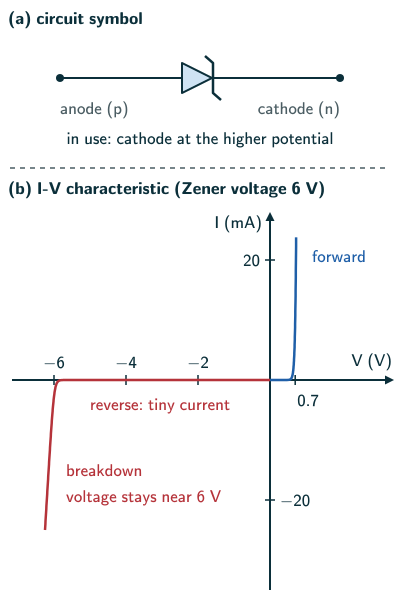
- Symbol: a diode symbol whose bar has bent ends; in use, the cathode (n-side) is connected to the higher potential (NEETS Module 7, Figure 3-4).
I-V characteristic and the reverse breakdown voltage
- Forward bias: a Zener diode behaves like an ordinary diode: little current until the threshold voltage, about 0.7 V for silicon, then a steep rise (reasoned from NCERT page 337).
- Reverse bias, below breakdown: the Manual gives an illustrative leakage of about 10−8 A to 10−10 A, too small for its meter. Actual leakage depends strongly on device, temperature and proximity to breakdown (Laboratory Manual, page 127).
- At breakdown: when the reverse voltage reaches VZ, the reverse current rises sharply. The voltage at which this happens is the Zener voltage, and the reverse current at that voltage is the Zener current (Laboratory Manual, page 126).
- Beyond breakdown: the curve is almost parallel to the current axis, so a very small change in voltage goes with a very large change in current (Laboratory Manual, page 126). Read the other way round, within the useful regulation range a large current change produces a small voltage change. Datasheets specify nominal VZ at a particular test current and temperature, not at every point of the knee. That is the property a regulator uses.
- The steepness is measured by the dynamic resistance rZ = ΔV/ΔI in the breakdown region, which is small (see Example 5). For an ideal Zener diode the line is vertical and rZ = 0 (reasoned from NCERT Eq. (14.6), page 337).
- The upper limit: the diode turns electrical energy into heat at the rate P = VZIZ, so its power rating PZ gives a nominal steady-state current limit at the stated temperature; apply any thermal derating and other ratings (Laboratory Manual, page 127):
Largest safe Zener current
- NCERT Figure 14.16(c) (page 336), the Laboratory Manual’s Fig. E 17.1 (page 126) and the figure below draw reverse values as negative, in the third quadrant. In the experiment the meters show Vr and Ir as positive numbers, and the Manual plots Vr along the x-axis and Ir along the y-axis (page 128).
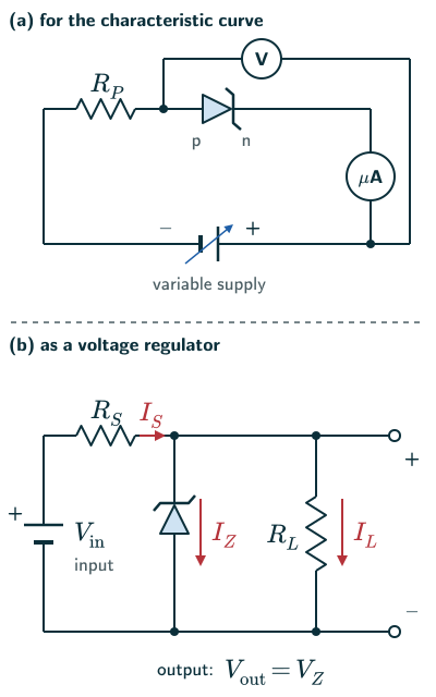
Circuit for the characteristic curve
- Aim (NCERT Laboratory Manual, Experiment 17, page 125): to draw the characteristic curve of a Zener diode and find its reverse breakdown voltage.
- Apparatus (page 125): a Zener diode, a variable dc supply (0–15 V), a microammeter (0–100 μA), a voltmeter (0–15 V), a protective resistance of 125 Ω, a high-resistance rheostat and connecting wires.
- Circuit (page 127): the Zener diode is connected in reverse bias, its n-side towards the positive terminal, in series with the protective resistance RP and the microammeter; the voltmeter goes across the diode. The rheostat is used as a potential divider across the supply, so that the reverse voltage can be raised from zero.
- Where the voltmeter goes (beyond the NCERT text): before breakdown the diode’s current is far smaller than the current a voltmeter draws, so a microammeter that also carries the voltmeter’s current would read the voltmeter, not the diode. Connect the voltmeter across the diode and microammeter together, as the figure shows; account for the microammeter’s burden voltage in that reading. The same connection tradeoff is discussed for an ordinary diode on the semiconductor diode page.
- Procedure (pages 127–128): check the zero of both meters. Raise the reverse voltage in steps of 0.1 V and note each voltmeter reading Vr and microammeter reading Ir. At first the microammeter reads zero; near breakdown the current starts to rise quickly. Connect the + terminal of each meter towards the + side of the supply (page 127). For the actual apparatus, choose a resistor or supply current limit that protects the meter as well as the diode. For a 15 V supply, a nominal 10 V diode and a 100 μA meter, even an ideal calculation needs at least (15 − 10)/100 μA = 50 kΩ, with extra margin for tolerances; use an appropriate mA range for mA data. Past the knee, raise the voltage slowly and stop before full scale: RP protects the diode, but in the Manual’s example it still allows (15 − 10)/125 = 40 mA, far beyond a 100 μA meter (reasoned).
- Graph and result (pages 128–129): plot Ir against Vr, with Vr along the x-axis, and read the breakdown voltage VZ from the graph, where the current shoots up. Small voltage steps near the knee locate it well (reasoned).
- Protective resistance (pages 126–127): after breakdown the diode alone would let the current grow without limit, so RP is put in series. With the full supply voltage V across the pair, V = VZ + IZRP; setting IZ to its largest safe value PZ/VZ gives the nominal minimum RP from the diode power alone (meter limits and component tolerances may require more):
Protective resistance (NCERT Laboratory Manual, Experiment 17)
- The Laboratory Manual’s example: a diode with VZ = 10 V and a power rating of 0.4 W, on a 15 V supply, needs RP = (15 − 10) × 10/0.4 = 125 Ω, the resistance in its apparatus list (page 127).
- Laboratory Manual slip (page 126): the Manual puts the diode and RP across a potential divider “with maximum potential VZ across it”, then writes V = VZ + IZRP. The maximum potential across the pair is the supply voltage V: with V = VZ, RP would be zero. Its own example uses V = 15 V.
- Precautions (page 129): clean the ends of the connecting wires with sandpaper, and check the zero readings of the voltmeter and microammeter.
Zener diode as a voltage regulator
- A dc supply made with a rectifier and capacitor filter is not perfectly steady: its voltage changes as the mains voltage and the load change. A voltage regulator holds the output steady. Zener diodes are most widely used as voltage regulators, because once breakdown is reached the voltage across the diode stays almost constant over the input range for which enough Zener current remains and its ratings are met (NEETS Module 7, page 3-7).
- The circuit: the unregulated input Vin feeds a series resistor RS. The Zener diode, reverse biased, is connected across the load RL, so the output voltage is the Zener voltage. NEETS calls this kind a shunt regulator, “because the regulating device is connected in parallel with the load resistance” (NEETS Module 7, page 4-38).
- The currents: the series resistor takes the voltage Vin − VZ, so its current is fixed by it; the load takes VZ/RL; and by the junction rule the Zener diode carries the rest:
Zener regulator currents
- First check that the diode is in breakdown. Take the diode out: the load would then get VinRL/(RS + RL). In the ideal constant-voltage model, only if this exceeds VZ can the diode regulate; a real device also needs its specified minimum regulation current. Otherwise the diode carries no current and the circuit is a potential divider (Example 3). In Example 1, 15 × 1000/1300 ≈ 11.5 V, well above 6.0 V (reasoned).
- If the input rises, IS rises. The extra current flows through the Zener diode, the output stays at VZ, and the extra voltage appears across RS. If the load draws more current, IZ falls by the same amount and the output again stays at VZ (reasoned; see Examples 2 and 3).
- Two limits (Wikipedia, “Zener diode”; the worst cases are reasoned):
- RS must be small enough that some current still flows through the diode and keeps it in breakdown when the input is lowest and the load current largest. With too little current, the output is no longer regulated and falls below VZ (Example 3).
- RS must be large enough that VZIZ never exceeds the diode’s power rating, the worst case being the highest input with the load disconnected.
- Zener diodes are also used to give fixed reference voltages in circuits and to protect circuits from overvoltage (Wikipedia, “Zener diode”).
For the ideal regulator examples, assume adequate Zener and resistor ratings unless a rating is explicitly tested. Real designs also check the minimum regulation current, test-current voltage, tolerances and thermal derating. Toshiba’s Zener explanation describes the two breakdown mechanisms.
Solved examples
Example 1: Currents in a regulator
A Zener diode with VZ = 6.0 V is used with RS = 300 Ω and a load of 1.0 kΩ on an input of 15 V. Find IS, IL, IZ and the power in the diode.
Answer: IS = (15 − 6.0)/300 = 30 mA; IL = 6.0/1000 = 6.0 mA; IZ = 30 − 6.0 = 24 mA. The diode dissipates VZIZ = 6.0 × 0.024 ≈ 0.14 W (reasoned).
Example 2: The input rises
In Example 1 the input rises to 18 V. Find the new currents and the output voltage.
Answer: IS = (18 − 6.0)/300 = 40 mA, IL is still 6.0 mA, so IZ = 34 mA. The output stays at 6.0 V: the extra 3 V appears across RS, and the extra 10 mA goes through the diode (reasoned).
Example 3: Too heavy a load
With the 15 V input and 300 Ω resistor of Example 1, what is the smallest load resistance that can be regulated? What is the output with a 150 Ω load?
Answer: IS = 30 mA at most, so the diode stays in breakdown only while IL < 30 mA: RL > 6.0/0.030 = 200 Ω (taking the smallest Zener current as zero). With 150 Ω the diode is not in breakdown and carries no current, so RS and RL share the input as a potential divider: Vout = 15 × 150/(300 + 150) = 5.0 V, below VZ (reasoned).
Example 4: Choosing the protective resistance
For the characteristic curve of a Zener diode with VZ = 8.2 V and a power rating of 0.50 W, the supply can reach 12 V. Find the largest safe current and the smallest safe RP.
Answer: IZ(max) = 0.50/8.2 ≈ 61 mA. RP = (12 − 8.2) × 8.2/0.50 = 62.32 Ω nominal minimum; rounding down to 62 Ω would slightly exceed 0.50 W. A nominal 68 Ω resistor gives about 55.9 mA and 0.458 W in the diode; check tolerances, resistor power and temperature derating before choosing a real part (NCERT Laboratory Manual, Experiment 17, Eq. (E 17.2), page 127).
Example 5: Dynamic resistance in breakdown
In breakdown, a Zener diode carries 10 mA at 6.00 V and 30 mA at 6.05 V. Find its dynamic resistance there.
Answer: rZ = ΔV/ΔI = 0.05/0.020 = 2.5 Ω. A 20 mA change in current moves the voltage by only 0.05 V, which is why the output of a regulator hardly changes (NCERT Eq. (14.6), page 337, applied to breakdown).
Common mistakes to avoid
Common mistake
Connecting the Zener diode forward biased
In a regulator the cathode (n-side) must go to the positive side. Forward biased, the diode holds only about 0.7 V, like any silicon diode.
Common mistake
Leaving out the series resistor
Beyond breakdown the diode itself does not limit the current; the external circuit must, using a resistor or another current limiter. Without it the diode overheats (NEETS Module 7, page 3-5).
Common mistake
Assuming the output is always the Zener voltage
The output equals VZ only while the diode is in breakdown. If the load needs more current than the series resistor supplies, the diode stops conducting and the circuit is a plain potential divider (Example 3).
Common mistake
Thinking breakdown always destroys a diode
Breakdown is reversible. A suitably rated Zener can survive breakdown while all current, temperature, power and pulse limits are respected (NCERT page 336; NEETS Module 7, page 3-5).
Quick revision summary
- A Zener diode is a purpose-designed p-n junction diode made to work in reverse breakdown; its symbol has a bent bar, and its cathode goes to the higher potential.
- Zener breakdown (tunnelling) usually dominates at low voltages, avalanche at higher voltages, with both contributing near the roughly 5–6 V crossover; both kinds are called Zener diodes.
- I-V curve: like an ordinary diode in forward bias; in reverse a tiny current until VZ, then an almost vertical rise in current at nearly constant voltage.
- The characteristic is taken with the diode in reverse bias, a protective resistor and a microammeter in series and a voltmeter across, raising the voltage in 0.1 V steps.
- As a regulator: series resistor RS, Zener diode reverse biased across the load; the output stays at VZ while the diode stays in breakdown and within its power rating.
Formula sheet
- IZ(max) = PZ/VZ
- RP = (V − VZ)VZ/PZ
- IS = (Vin − VZ)/RS
- IL = VZ/RL
- IZ = IS − IL
- rZ = ΔV/ΔI
Questions students ask
Is the Zener diode in the JEE Main and NEET syllabus?
Yes, the Zener diode is in both syllabuses: Unit 19, Electronic Devices, of the JEE Main syllabus and of the NEET (UG) 2026 syllabus lists the I-V characteristic of the Zener diode and the “Zener diode as a voltage regulator”, and Unit 20 of both has the experiment “Characteristic curves of a Zener diode and finding reverse breakdown voltage” (JEE wording). The current NCERT Class 12 Physics Part II, still the 2025–26 reprint, has no section on it: page 337 says this special breakdown action “is discussed later in Section 14.8”, a section the reprint lacks. The experiment is Experiment 17 of the NCERT Laboratory Manual (Physics, Class 12), pages 125–129.
How is a Zener diode different from an ordinary p-n junction diode?
A Zener diode differs from an ordinary p-n junction diode in being more heavily doped on both sides and in being made to dissipate enough power to work in the reverse breakdown region (NCERT Laboratory Manual, Physics, Class 12, page 125). Beyond the NCERT text, its doping sets its breakdown voltage, anywhere from about 2 V to 200 V (US Navy, NEETS Module 7, page 3-5); in breakdown its voltage stays nearly constant, so it is used there as a regulator, whereas NCERT says general-purpose diodes are not used beyond the reverse saturation region (page 337). In forward bias the two behave alike (reasoned), conducting beyond the silicon threshold of about 0.7 V that NCERT gives on page 337.
What is the difference between Zener breakdown and avalanche breakdown?
Zener breakdown and avalanche breakdown differ, beyond the NCERT text, in how carriers are freed: in Zener breakdown the field of a very thin, heavily doped junction lets valence electrons tunnel across, while in avalanche breakdown accelerated carriers break bonds in collisions and free more in a chain (US Navy, NEETS Module 7, pages 3-3 to 3-5). In silicon the Zener effect tends to dominate below roughly 5 V and avalanche above roughly 6 V, with both contributing between them, and heat acts on them oppositely: a Zener-effect diode’s breakdown voltage falls as the temperature rises, an avalanche diode’s rises (Wikipedia, “Zener diode”). Close to 5.6 V both act and offset each other, so a suitably chosen device and operating current can have a small temperature coefficient; cancellation is not exact for every nominal 5.6 V diode.
Is the Zener voltage the same as the breakdown voltage?
Yes, for a Zener diode the Zener voltage VZ is its reverse breakdown voltage: the NCERT Laboratory Manual (Physics, Class 12) gives the name Zener voltage to the voltage at which breakdown occurs (page 126). Beyond the NCERT text, makers set VZ by the doping, with a tolerance commonly of 5% or 10% (Wikipedia, “Zener diode”), so a diode sold as 7.5 V with a 5% tolerance has a specified voltage range 7.125 V to 7.875 V at the datasheet’s test current and temperature. The onset of the knee and voltages at other currents are not identical to that tolerance range. For an ordinary diode the breakdown voltage is instead a limit that the reverse voltage must stay below.
How does a Zener diode protect a circuit from overvoltage?
A Zener diode protects a circuit from overvoltage, a use beyond the NCERT text that Wikipedia’s “Zener diode” lists, when it is connected reverse biased across the circuit’s supply or input with a Zener voltage a little above the normal working voltage (reasoned). At normal voltages it stays below breakdown and draws only a tiny reverse current, but a spike that would push the voltage past VZ drives it into breakdown, so it conducts heavily and holds the voltage near VZ (reasoned). A series resistance must take up the excess voltage and limit the diode’s current (reasoned), and two Zener diodes joined back to back clip spikes of either sign (Wikipedia).
Why is a Zener diode not used as a rectifier?
A Zener diode is not used as a rectifier because, beyond the NCERT text, it is built to break down and conduct in reverse at its Zener voltage: in the half-cycles it should block, any reverse voltage above VZ drives it into breakdown and current flows backwards through the load (reasoned). A rectifier diode must withstand the whole reverse voltage across it, in a centre-tap rectifier twice the peak of each half of the secondary (rectifier Example 4). As long as that reverse voltage stays below VZ, a Zener diode would rectify like an ordinary diode (reasoned).
Practice questions
Try each question first, then open the answer to check your working.
-
Q1. Why is the Zener diode in a voltage regulator connected in reverse bias?
Show answerHide answer
Only in reverse breakdown does the voltage across it stay almost constant at VZ as the current changes. Forward biased, it would hold only about 0.7 V, like an ordinary silicon diode.
-
Q2. A 5.1 V Zener diode has a power rating of 0.50 W. What is the largest current it can safely carry?
Show answerHide answer
IZ(max) = PZ/VZ = 0.50/5.1 ≈ 0.098 A, about 98 mA (NCERT Laboratory Manual, page 127).
-
Q3. A regulator has Vin = 20 V, VZ = 9.0 V, RS = 220 Ω and RL = 1.5 kΩ. Find the current through the Zener diode.
Show answerHide answer
IS = (20 − 9.0)/220 = 50 mA; IL = 9.0/1500 = 6.0 mA; so IZ = 50 − 6.0 = 44 mA.