Extrinsic semiconductor
NCERT Class 12 Physics Chapter 14 Section 14.4
Quick answer
An extrinsic semiconductor has a carrier population controlled by dopants; in Si and Ge, pentavalent donors give n-type material and trivalent acceptors give p-type material. Electrons are the n-type majority carriers, holes the p-type majority carriers, and the bulk remains electrically neutral. In nondegenerate thermal equilibrium ne nh = ni2.
With your textbook
NCERT Physics Part II (Class 12), Chapter 14 “Semiconductor Electronics: Materials, Devices and Simple Circuits”, Section 14.4 “Extrinsic Semiconductor”, pages 329–332.
Open the official NCERT chapter (PDF, 1.9 MB, ncert.nic.in) (opens in a new tab)
Checked against the 2025-26 reprint on .
What is an extrinsic semiconductor?
Extrinsic semiconductor
An extrinsic semiconductor is a pure semiconductor, such as silicon or germanium, to which a small amount of a suitable impurity, say a few parts per million, has been added, increasing its conductivity manifold (NCERT page 329). It is also called an impurity or doped semiconductor. In NCERT’s words:
The deliberate addition of a desirable impurity is called doping and the impurity atoms are called dopants.
NCERT Physics Part II (Class 12), Section 14.4, page 329
Pentavalent dopants such as arsenic give n-type material, in which electrons are the majority carriers; trivalent dopants such as boron give p-type material, in which holes are the majority carriers (NCERT pages 330–331).
In plain words: pure silicon has few free carriers at room temperature; doping allows their density and dominant type to be controlled. Swap about one silicon atom in a million for an atom with one electron more, and that spare electron is almost free; swap it for an atom with one electron fewer, and a bond is left one electron short, a hole. Either way the number of carriers jumps, and you choose which kind.
Doping
- The conductivity of an intrinsic semiconductor depends on its temperature, but at room temperature it is very low: “no important electronic devices can be developed using these semiconductors”, so impurities are added to raise it (NCERT page 329). Strictly, doping also gives a controlled population of majority carriers (reasoned).
- Adding a few parts per million (ppm) of a suitable impurity increases the conductivity manifold (NCERT page 329).
- Suitable substitutional dopants replace host atoms without destroying the crystal. In NCERT’s words, the dopant “has to be such that it does not distort the original pure semiconductor lattice”, and a necessary condition is that the sizes of the dopant and the semiconductor atoms “should be nearly the same” (NCERT page 329).
- Si and Ge belong to the fourth group of the periodic table (group 14 today), so dopants are chosen from the nearby fifth and third groups (NCERT page 330):
- pentavalent (valency 5): arsenic (As), antimony (Sb), phosphorus (P);
- trivalent (valency 3): indium (In), boron (B), aluminium (Al).
n-type semiconductor and donors
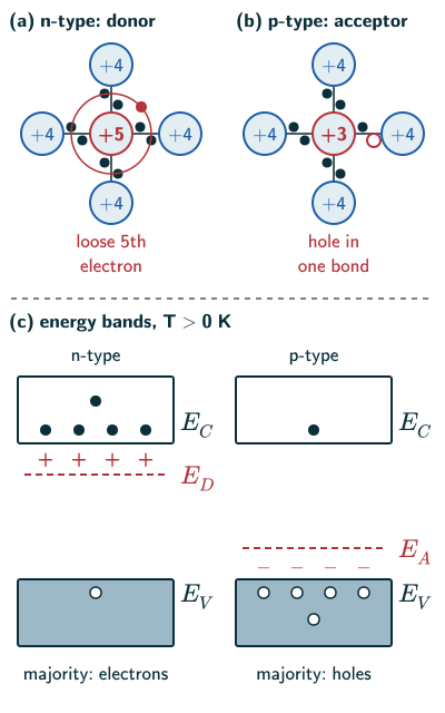
- When a pentavalent atom takes the place of a Si atom, four of its five valence electrons form bonds with the four silicon neighbours. The fifth is only very weakly bound to its parent atom, because it sees the four bonding electrons as part of the atom’s effective core (NCERT page 330, NCERT Figure 14.7(a)).
- So very little energy sets the fifth electron free: about 0.01 eV in germanium and 0.05 eV in silicon, against about 0.72 eV and 1.1 eV to jump the forbidden band. Even at room temperature it is free to move through the lattice (NCERT page 330).
- The pentavalent atom donates an electron for conduction, so it is a donor impurity. The number of electrons the donors supply depends strongly on the doping level and, since nearly all donors are already ionised at room temperature, hardly grows as the crystal warms further; NCERT says “independent of any increase in ambient temperature” (page 330).
- NCERT slip (page 330): NCERT adds that the number of electron-hole pairs generated by the Si atoms themselves “increases weakly with temperature”. The equilibrium intrinsic carrier concentration rises steeply: NCERT Chapter 3 (page 91) explains that the number of carriers in a semiconductor grows so fast with temperature that its resistivity falls as it warms, and the current in an intrinsic semiconductor is highly temperature dependent (Wikipedia, “Intrinsic semiconductor”).
- The conduction electrons come from the donors and from intrinsic generation; the holes come only from intrinsic generation. With so many more electrons, holes recombine faster, so the number of holes falls even below its intrinsic value (NCERT page 330).
- Electrons are the majority carriers and holes the minority carriers: this is an n-type semiconductor (NCERT Eq. (14.3), page 331):
n-type semiconductor (NCERT Eq. 14.3)
- NCERT Figure 14.7(b) draws n-type material as fixed donor cores, each with one extra positive charge, and their extra electrons (NCERT page 330).
p-type semiconductor and acceptors
- A trivalent atom such as Al, B or In has one valence electron fewer than Si. It forms covalent bonds with three Si neighbours but has no electron to offer the fourth, so that bond has a vacancy, a hole (NCERT page 331, NCERT Figure 14.8(a)).
- An electron from a neighbouring atom may jump into this vacancy, leaving a hole at its own site, so the hole is available for conduction (NCERT page 331).
- Once it has taken this fourth electron, the trivalent atom is effectively negatively charged: NCERT Figure 14.8(b) draws it as a core of one negative charge with its hole. One acceptor gives one hole, so the dopant is an acceptor (NCERT page 331).
- The holes from the acceptors add to the intrinsic holes, while the only source of conduction electrons is intrinsic generation; recombination cuts the electrons below ni. Holes are the majority carriers and electrons the minority carriers: this is a p-type semiconductor (NCERT Eq. (14.4), page 331):
p-type semiconductor (NCERT Eq. 14.4)
- The crystal stays neutral. The charge of the extra carriers is equal and opposite to that of the ionised dopant cores fixed in the lattice (NCERT page 331).
- With so many majority carriers about, the thermally produced minority carriers are more likely to meet one and be destroyed. So by adding carriers of one kind, the dopant indirectly lowers the number of the other kind (NCERT page 331).
Energy bands of doped semiconductors
- Doping adds energy states: donor levels ED and acceptor levels EA (NCERT page 331).
- In n-type Si the donor level ED lies slightly below the bottom EC of the conduction band, so a very small supply of energy lifts its electrons into the conduction band. At room temperature most donor atoms are ionised but very few Si atoms are, so most conduction electrons come from the donors (NCERT page 331, NCERT Figure 14.9(a)).
- NCERT Figure 14.9(a), which the text uses for n-type Si, marks the donor level about 0.01 eV below EC, the germanium value; for silicon NCERT’s text gives 0.05 eV (page 330).
- NCERT gives the number of ionised Si atoms as “(~1012)” (page 331), with no unit or volume. The bare number cannot be a concentration without units. For comparison, in pure Si, NCERT Example 14.2’s 1.5 × 10¹⁶ pairs among 5 × 1028 atoms m−3 gives about one conduction electron per 3.3 × 10¹² atoms. In the doped example the equilibrium hole density is only 4.5 × 10⁹ m−3. These are mobile-carrier population ratios, not a permanent census of ionised Si atoms.
- In p-type Si the acceptor level EA lies slightly above the top EV of the valence band. A very small supply of energy lets an electron from the valence band jump to EA, ionising the acceptor; equivalently, the hole sinks from EA into the valence band. At room temperature most acceptors are ionised, so the holes in the valence band come mainly from the impurity (NCERT page 332, NCERT Figure 14.9(b)).
- In thermal equilibrium in the nondegenerate regime, in intrinsic, n-type and p-type material alike, the electron and hole concentrations obey (NCERT Eq. (14.5), page 332; NCERT Summary point 9, page 340):
Electron and hole concentrations (NCERT Eq. 14.5)
- NCERT calls this band picture “grossly approximate and hypothetical”, but useful for seeing how metals, insulators and semiconductors differ (NCERT page 332).
- Conductivity (beyond the NCERT text): as in pure silicon, σ = e(neμe + nhμh), where μe and μh are the mobilities. In n-type material the holes add almost nothing, so σ ≈ eneμe. See Example 3.
The numerical examples assume thermal equilibrium, moderate nondegenerate doping, full shallow-dopant ionisation and negligible compensation unless stated. At very low temperatures dopants can freeze out; at high temperatures intrinsic carriers can dominate.
Solved examples
Example 1: Doping silicon with arsenic (NCERT Example 14.2)
A pure Si crystal has 5 × 1028 atoms m−3. It is doped with 1 ppm of pentavalent As. Find the numbers of electrons and holes, given ni = 1.5 × 10¹⁶ m−3.
Answer: One part per million of the atoms are donors: ND = 5 × 1028/106 = 5 × 10²² m−3. Assuming full donor ionisation and no compensating acceptors, charge neutrality gives ne − nh = ND. Since ND ≫ ni, the minority contribution is negligible, so ne ≈ 5 × 10²² m−3. Then nh = ni2/ne = (2.25 × 1032)/(5 × 1022) ≈ 4.5 × 10⁹ m−3, far fewer holes than in pure silicon (NCERT Example 14.2, page 332).
Example 2: n-type silicon (NCERT Exercises 14.1–14.2)
In n-type silicon, which is true? (a) Electrons are majority carriers and trivalent atoms are the dopants. (b) Electrons are minority carriers and pentavalent atoms are the dopants. (c) Holes are minority carriers and pentavalent atoms are the dopants. (d) Holes are majority carriers and trivalent atoms are the dopants. Which statement is true for p-type silicon?
Answer: For n-type, (c): pentavalent donors make electrons the majority, so holes are the minority. For p-type, (d) (NCERT pages 330–331; NCERT answers, page 352).
Example 3: How much does doping help?
Taking μe = 0.135 m2 V−1 s−1, its value in pure silicon (doping lowers it, so this is an upper estimate), find the conductivity of the doped silicon of Example 1, and compare it with that of pure silicon, about 4.4 × 10⁻⁴ S m−1.
Answer: σ ≈ eneμe = 1.6 × 10−19 × 5 × 1022 × 0.135 ≈ 1.1 × 10³ S m−1, about 2.5 × 10⁶ times that of pure silicon, from one impurity atom in a million (beyond the NCERT text).
Example 4: Doping silicon with boron
The same silicon is doped instead with 2 ppm of boron. Find nh and ne.
Answer: NA = 2 × 5 × 1028/106 = 1023 m−3, so nh ≈ 1023 m−3 and ne = (2.25 × 1032)/1023 = 2.25 × 10⁹ m−3 (worked as NCERT Example 14.2, page 332).
Example 5: Why are donor electrons free at room temperature?
Freeing a donor electron in silicon takes about 0.05 eV, but breaking a bond takes about 1.1 eV. Compare each with kT at 300 K.
Answer: kT = 1.38 × 10−23 × 300/(1.6 × 10−19) ≈ 0.026 eV. This scale comparison makes donor ionisation much easier than interband excitation. It does not by itself calculate the ionised fraction; carrier statistics and doping matter. For ordinary shallow, moderately doped Si donors NCERT takes most as ionised at room temperature (page 331). But 1.1 eV is over 40 kT, so very few bonds break (energies from NCERT page 330; kT beyond the NCERT text).
Common mistakes to avoid
Common mistake
Thinking n-type material is negatively charged
The extra electrons are matched by the positive donor ions fixed in the lattice, so the crystal is neutral; n stands for the sign of the majority carriers (NCERT page 331).
Common mistake
Thinking doping raises both kinds of carrier
Doping raises the majority carriers but lowers the minority carriers below ni, because they recombine faster (NCERT pages 330–331; Example 1).
Common mistake
Mixing up donors and acceptors
Pentavalent atoms (As, Sb, P) donate an electron: n-type. Trivalent atoms (B, Al, In) accept one: p-type (NCERT pages 330–331).
Quick revision summary
- Doping a few ppm of a suitable impurity raises a semiconductor’s conductivity manifold; the dopant must not distort the lattice, so its atoms must be nearly the same size as the host atoms.
- Pentavalent donors (As, Sb, P) give n-type: electrons are the majority carriers, ne ≫ nh.
- Trivalent acceptors (B, Al, In) give p-type: holes are the majority carriers, nh ≫ ne.
- Donor levels lie just below EC, acceptor levels just above EV; at room temperature most dopants are ionised.
- In nondegenerate thermal equilibrium nenh = ni2; the crystal is electrically neutral.
Formula sheet
- ne ≫ nh (n-type)
- nh ≫ ne (p-type)
- ne nh = ni2
- σ = e(ne μe + nh μh)
Questions students ask
What is the difference between n-type and p-type semiconductors?
An n-type semiconductor is silicon or germanium doped with a pentavalent donor, so electrons are the majority carriers and the fixed donor ions are positive, while a p-type semiconductor is doped with a trivalent acceptor, so holes are the majority carriers and the fixed acceptor ions are negative (NCERT pages 330–331). Their extra energy levels sit at opposite edges of the gap: the donor level just below the conduction band, the acceptor level just above the valence band (NCERT pages 331–332). Beyond the NCERT text, for the same doping level n-type silicon conducts better, because electrons are roughly three times as mobile as holes (Wikipedia, “Electron mobility”).
Why is doping necessary in semiconductors?
Doping is necessary because a pure semiconductor’s conductivity at room temperature is too low for any important electronic device, while a few parts per million of a suitable impurity raises it many times (NCERT page 329). Beyond the NCERT text, undoped (intrinsic) layers still have uses, as in p-i-n diodes for light and radiation detectors (Wikipedia, “Diode”). Doping also chooses the majority carrier, electrons in n-type or holes in p-type, and joining the two makes a p-n junction. Once nearly all donors are ionised, as at room temperature, the electrons they supply hardly change with temperature (NCERT pages 330–331), while a pure crystal’s carriers multiply as it warms (reasoned).
What is the mass action law in semiconductors, and why does it hold?
The mass action law in semiconductors says that in nondegenerate thermal equilibrium the product of the electron and hole concentrations is fixed at a given temperature, nenh = ni2, in pure, n-type and p-type material alike (NCERT Eq. (14.5), page 332). In the nondegenerate band model, ne ∝ exp[(EF − EC)/kT] and nh ∝ exp[(EV − EF)/kT]; multiplying cancels the common equilibrium Fermi energy EF. This does not assume every recombination mechanism is simply proportional to np. Strong degeneracy or nonequilibrium illumination needs a more general treatment (Wikipedia, “Charge carrier density” and “Carrier generation and recombination”). So silicon with ne = 3 × 10 m and ni = 1.5 × 10 m has nh = 7.5 × 10 m.
What is doping concentration, and how is it calculated?
Doping concentration is the number of dopant atoms per unit volume of the crystal, ND for donors or NA for acceptors, in m (books that use cm give numbers 10 times smaller); it is the fraction of host atoms replaced times the number of host atoms per unit volume, as in NCERT Example 14.2 (page 332). For silicon, with 5 × 10 atoms m, doping with one phosphorus atom in 10 gives ND = 5 × 10 m, and at room temperature most of these donors are ionised (NCERT page 331). “Light” and “heavy” doping are relative to the material and application; there is no universal ppm boundary.
Why are pentavalent and trivalent impurities commonly used to dope silicon?
Pentavalent and trivalent impurities are used because each has one valence electron more or fewer than silicon, so each atom supplies one loosely bound electron or hole that is freed at room temperature (NCERT pages 330–332). Beyond the NCERT text, other impurities such as gold make levels deep in the band gap that capture carriers rather than supply them, and gold is added to some silicon devices to shorten carrier lifetimes (Wikipedia, “Doping (semiconductor)”). In compound semiconductors a foreign atom is not the only way: native defects and departures from stoichiometry can also affect carriers. NCERT’s Ga-rich/As-rich illustration (Points to ponder 2, page 341) is qualitative, not a recipe for a homogeneous Ga1.1As0.9 crystal.
Practice questions
Try each question first, then open the answer to check your working.
-
Q1. Why is a pentavalent impurity in silicon called a donor?
Show answerHide answer
Four of its five valence electrons form bonds; the fifth is so weakly bound that it is freed at room temperature, so the atom donates an electron for conduction (NCERT page 330).
-
Q2. Where does the acceptor level lie in the band diagram of p-type silicon, and what happens at room temperature?
Show answerHide answer
Slightly above the top of the valence band, EV. Valence electrons easily jump to it, so most acceptors are ionised and holes are left in the valence band (NCERT page 332).
-
Q3. A Si sample is doped so that ne = 1022 m−3. With ni = 1.5 × 10¹⁶ m−3, find nh.
Show answerHide answer
nh = ni2/ne = (2.25 × 1032)/1022 = 2.25 × 10¹⁰ m−3 (NCERT Eq. (14.5), page 332).