p-n junction
NCERT Class 12 Physics Chapter 14 Section 14.5
Quick answer
A p-n junction is the boundary between p-type and n-type regions in a continuous crystal. Carrier diffusion leaves a depletion region of fixed ionised dopants, whose field points from n to p and opposes diffusion. At thermal equilibrium drift and diffusion currents balance, and the n-side is at a higher internal potential; width depends on doping and bias.
With your textbook
NCERT Physics Part II (Class 12), Chapter 14 “Semiconductor Electronics: Materials, Devices and Simple Circuits”, Section 14.5 “p-n Junction”, pages 333–334.
Open the official NCERT chapter (PDF, 1.9 MB, ncert.nic.in) (opens in a new tab)
Checked against the 2025-26 reprint on .
What is a p-n junction?
p-n junction
A p-n junction is the boundary, inside a single crystal, between a p-type region and an n-type region. In NCERT’s words:
A p-n junction is the basic building block of many semiconductor devices like diodes, transistor, etc.
NCERT Physics Part II (Class 12), Section 14.5, page 333
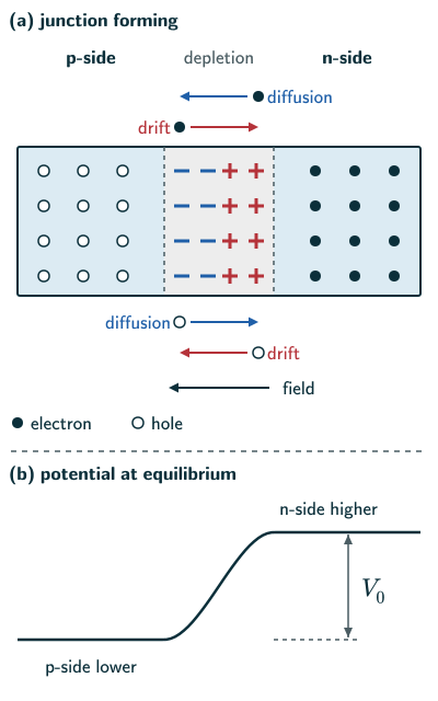
As the junction forms, electrons and holes diffuse across it and leave behind a thin depletion region of fixed ions. The field of these ions drives a drift current the other way. At thermal equilibrium the two opposite currents have equal magnitudes, so no net current flows, and the n-side is at a higher potential than the p-side: the barrier potential (NCERT pages 333–334).
In plain words: put a region crowded with free electrons next to one crowded with holes, and each kind spreads into the other side, as ink spreads in water. But every carrier that crosses leaves a charged atom behind, fixed in the crystal. These charges build up a field that pushes carriers back. Soon the push back exactly balances the spreading, and the junction settles down with a small voltage across it.
p-n junction formation
- Start with a thin wafer of p-type silicon. Adding a precise, small amount of pentavalent impurity to part of it, enough for the donors there to outnumber the acceptors, turns that part into n-type silicon. The wafer now has a p-region, an n-region and a metallurgical junction between them (NCERT page 333).
- For the ordinary homojunction discussed here, the two regions are made within a continuous crystal. Simply pressing two separate slabs together will not do, because their surfaces are far rougher than the spacing of the atoms (NCERT Example 14.3, page 334; see Example 1).
- Two processes take place while the junction forms: diffusion and drift (NCERT page 333).
Diffusion and drift
- In n-type material the concentration of electrons (their number per unit volume) is greater than that of holes; in p-type material the concentration of holes is greater (NCERT page 333).
- Because of this concentration gradient, holes diffuse from the p-side to the n-side, and electrons from the n-side to the p-side. This motion of carriers is the diffusion current across the junction (NCERT page 333).
- The charged layers left behind (see Depletion region) set up an electric field. It makes an electron on the p-side of the junction move to the n-side, and a hole on the n-side move to the p-side. Motion of carriers due to a field is called drift, as with the drift of electrons in a wire, and this drift current is opposite in direction to the diffusion current (NCERT page 333, NCERT Figure 14.10).
- Which way the currents flow (reasoned): electrons moving n → p and holes moving p → n both carry conventional current from p to n, so the diffusion current flows from p to n and the drift current from n to p.
- Introductory current picture: majority-carrier injection is associated with diffusion, and minority carriers swept across the depletion region give the reverse drift component. Both drift and diffusion terms can, more generally, contribute to each carrier species; the field does not act only on minority carriers. The drift is carried by the few electrons on the p-side and holes on the n-side, which is why NCERT later calls the drift current “quite low” (page 335).
- At first the diffusion current is large and the drift current small. As diffusion goes on, the charged layers grow, the field strengthens and the drift current rises, until the drift current equals the diffusion current (NCERT page 334). In NCERT’s words:
This process continues until the diffusion current equals the drift current.
NCERT Physics Part II (Class 12), Section 14.5.1, page 334
At equilibrium (NCERT page 334)
- So in a p-n junction at equilibrium there is no net current (NCERT page 334).
Depletion region
- When an electron diffuses from n to p, it leaves behind an ionised donor, a positive charge. This ion cannot move, because it is bonded to the surrounding atoms. As more electrons diffuse, a layer of positive charge, a positive space-charge region, builds up on the n-side of the junction (NCERT page 333).
- In the same way, each hole that diffuses from p to n leaves behind an immobile ionised acceptor, a negative charge, building a negative space-charge region on the p-side (NCERT page 333).
- The two space-charge regions together are the depletion region: the carriers that crossed at first have depleted it of free charges (NCERT page 333, NCERT Figure 14.10).
- Its thickness is of the order of one-tenth of a micrometre, 10−7 m (NCERT page 333; see Example 4). Strictly, it depends on the doping and on the bias: it narrows in forward bias and widens in reverse bias (NCERT pages 334–335), and heavier doping makes it thinner (see Typical sizes below).
- The positive charge on the n-side and the negative charge on the p-side set up an electric field from the n-side towards the p-side, from positive charge towards negative (NCERT page 333).
Barrier potential
- The n-region has lost electrons and the p-region has gained them, so a potential difference develops across the junction. Its polarity opposes further diffusion, of electrons from n to p and holes from p to n, so a condition of equilibrium exists (NCERT page 334); the same field drives the drift.
- The n-material is therefore positive relative to the p-material. Since this potential tends to stop electrons moving from the n-region into the p-region, it is called the barrier potential (NCERT page 334, NCERT Figure 14.11). NCERT Figure 14.11 labels it V0 and the depletion width W; the text calls V0 the built-in potential (page 335).
- Typical sizes (beyond the NCERT text): V0 is a few tenths of a volt, of the order of the threshold voltages NCERT gives for diodes, about 0.7 V for silicon and 0.2 V for germanium (page 337); Wikipedia’s “P–n junction” gives about 0.59 V for one example junction, doped at 1021 m−3 on both sides. The charges on the two sides of the junction are equal and opposite, so the depletion region reaches further into the more lightly doped side (Wikipedia, “P–n junction”). Heavier doping gives a thinner depletion region, less than 10−7 m across in a Zener diode (NCERT Laboratory Manual, Physics, Class 12, page 125).
- How strong is the field? (beyond the NCERT text): a potential difference V0 across a depletion region of width W gives an average field of about V0/W, the size of the potential gradient. Because W is so small, this field is very large (see Example 3).
Average field in the depletion region (beyond the NCERT text)
The built-in voltage is an internal electrostatic potential difference, not a battery emf available at equilibrium terminals. Contact potential differences balance in a complete measurement circuit, so an unbiased junction cannot deliver continuous power.
Solved examples
Example 1: Two slabs pressed together (NCERT Example 14.3)
Can we take one slab of p-type semiconductor and physically join it to another of n-type to get a p-n junction?
Answer: No. However flat they are, the slabs have surface roughness much larger than the inter-atomic spacing of the crystal, about 2 to 3 Å, so they cannot be in continuous contact at the atomic level. The join would act as a discontinuity for the charge carriers (NCERT Example 14.3, page 334).
Example 2: Why holes diffuse (NCERT Exercise 14.4)
In an unbiased p-n junction, holes diffuse from the p-region to the n-region because (a) free electrons in the n-region attract them; (b) they move across the junction by the potential difference; (c) the hole concentration in the p-region is more than in the n-region; (d) all of the above.
Answer: (c). Diffusion is driven by the difference in concentration. The potential difference across the junction in fact opposes the holes (NCERT pages 333–334; NCERT Exercise 14.4, page 342; answer on page 352).
Example 3: The field across the depletion region
Taking a barrier potential of 0.6 V across a depletion region 0.1 μm wide, find the average field in it and compare it with the dielectric strength of air, about 3 × 10⁶ V m−1.
Answer: E ≈ V0/W = 0.6/10−7 = 6 × 10⁶ V m−1, twice the field at which air breaks down (width from NCERT page 333; dielectric strength from NCERT Chapter 2, page 68; the rest beyond the NCERT text).
Example 4: How many atoms wide?
The depletion region is about 0.1 μm thick, and the inter-atomic spacing is about 2 to 3 Å. Roughly how many atomic spacings wide is it?
Answer: 0.1 μm = 1000 Å, so about 1000/3 ≈ 330 to 1000/2 = 500 spacings (NCERT pages 333–334).
Example 5: Directions of the currents
In a junction with the p-side on the left, which way do the diffusion current, the drift current and the field point?
Answer: Diffusion current: p to n, to the right. Drift current: n to p, to the left. Field: from the positive ions on the n-side to the negative ions on the p-side, to the left (field from NCERT page 333; current directions reasoned).
Common mistakes to avoid
Common mistake
Thinking the depletion region holds no charge
It is depleted of free charges, but holds fixed charge: positive donor ions on the n-side and negative acceptor ions on the p-side (NCERT page 333). Strictly, a few mobile carriers remain; the depletion approximation neglects them (reasoned).
Common mistake
Thinking no current flows in an unbiased junction
Diffusion and drift currents both flow; at equilibrium they are equal and opposite, so the net current is zero (NCERT page 334).
Common mistake
Pointing the junction field from p to n
The field runs from the positive ions on the n-side to the negative ions on the p-side, so it points from n to p (NCERT page 333).
Quick revision summary
- A p-n junction is made inside one crystal by doping part of a p-type wafer n-type.
- Diffusion: holes go p → n and electrons n → p, down their concentration gradients.
- They leave fixed ions: + on the n-side, − on the p-side, forming a depletion region about 0.1 μm thick.
- Its field, from n to p, drives a drift current opposite to the diffusion current; at equilibrium Idiffusion = Idrift and the net current is zero.
- The n-side is at a higher potential than the p-side by the barrier potential V0; E ≈ V0/W (beyond the NCERT text).
Formula sheet
- Idiffusion = Idrift (equilibrium)
- E ≈ V0/W
Questions students ask
What is the difference between diffusion current and drift current in a p-n junction?
Diffusion current in a p-n junction is the flow of majority carriers down their concentration gradient, holes from p to n and electrons from n to p, so it runs from p to n, while drift current is the flow of minority carriers, electrons on the p-side and holes on the n-side, swept across by the junction’s field, so it runs from n to p (NCERT page 333; directions reasoned). In an unbiased junction the two are equal (NCERT page 334); forward bias lowers the barrier and the diffusion current grows to mA, while reverse bias leaves only a drift current of a few μA (NCERT page 335).
What is the difference between the depletion region and the barrier potential?
The depletion region is the layer on both sides of the junction strongly depleted of mobile electrons and holes, so fixed ionised dopants dominate its space charge, while the barrier potential V0 is the potential difference these ions set up across it (NCERT pages 333–334). One is a region, the other a voltage; a bias changes both together (NCERT page 335). Beyond the NCERT text, an abrupt junction has a width W = √[2ε(V0 + V)(1/NA + 1/ND)/e], within the abrupt-junction depletion approximation, with fully ionised dopants and before breakdown, for reverse-bias magnitude V, permittivity ε and acceptor and donor concentrations NA and ND, so the layer is thinner for heavier doping and widens with reverse bias (Wikipedia, “P–n junction”).
What is the formula for the barrier potential, and what is it for silicon and germanium?
For a nondegenerate homojunction at equilibrium with fully ionised dopants, the barrier potential is V0 = (kT/e) ln(NAND/ni2), beyond the NCERT text, for acceptor and donor concentrations NA and ND (Wikipedia, “P–n junction”); NCERT gives no formula. With 2 × 10 m of each at 300 K (kT/e ≈ 0.0259 V), it gives about 0.73 V for silicon (NCERT’s ni = 1.5 × 10 m, page 332) but 0.36 V for germanium (ni ≈ 2 × 10 m, Ioffe Institute; why silicon is preferred). It rises slowly with doping and falls as the temperature rises (reasoned).
What is the difference between a p-n junction and a p-n junction diode?
A p-n junction is the boundary inside one crystal between its p-type and n-type regions, where the depletion region and barrier form, while a p-n junction diode is that junction made into a device, with a metal contact at each end so that a voltage can be applied (NCERT pages 333–334). The diode is a two-terminal device (NCERT page 334); how it behaves in forward and reverse bias is in NCERT Section 14.6 (pages 334–337). Every p-n junction diode contains such a junction; semiconductor diodes also include metal–semiconductor devices such as Schottky diodes, but NCERT calls the junction the building block of other devices too, such as transistors (page 333).
Is the p-n junction in the JEE Main and NEET syllabus?
Yes, the p-n junction is in both syllabuses through the diode: Unit 19, Electronic Devices, of the JEE Main syllabus and of the NEET (UG) 2026 syllabus lists the “semiconductor diode: I-V characteristics in forward and reverse bias”, and Unit 20 of both has the experiment “Characteristic curves of a p-n junction diode in forward and reverse bias.” Neither names the depletion region or barrier potential, but the diode cannot be explained without them. NCERT Class 12 Physics Part II covers the junction in Section 14.5 (pages 333–334) of the 2025–26 reprint.
Practice questions
Try each question first, then open the answer to check your working.
-
Q1. Why are the ions in the depletion region unable to move?
Show answerHide answer
They are donor and acceptor atoms bonded to the surrounding atoms of the crystal; only the electrons and holes they gave up or took in can move (NCERT page 333).
-
Q2. In an unbiased p-n junction, which side is at the higher potential, and why?
Show answerHide answer
The n-side. It has lost electrons to the p-side, leaving fixed positive donor ions, while the p-side has gained electrons (NCERT page 334).
-
Q3. While a junction is forming, what happens to the drift current, and when does it stop changing?
Show answerHide answer
It grows as the space-charge layers and their field grow, until it equals the diffusion current; then the junction is at equilibrium (NCERT page 334).