Semiconductor diode
NCERT Class 12 Physics Chapter 14 Section 14.6
Quick answer
A p-n junction diode conducts much more readily in forward bias, with p-side positive, than in reverse bias below breakdown. The junction barrier is approximately V0 − V in forward bias and V0 + V in reverse bias; the familiar 0.7 V silicon knee is approximate and depends on current and temperature. Dynamic resistance is rd = ΔV/ΔI for small changes near an operating point.
With your textbook
NCERT Physics Part II (Class 12), Chapter 14 “Semiconductor Electronics: Materials, Devices and Simple Circuits”, Section 14.6 “Semiconductor Diode”, pages 334–337.
Open the official NCERT chapter (PDF, 1.9 MB, ncert.nic.in) (opens in a new tab)
Checked against the 2025-26 reprint on .
What is a semiconductor diode?
Semiconductor diode
The p-n junction semiconductor diode studied here is a p-n junction with a metal contact at each end, so that a voltage can be applied across it: a two-terminal device (NCERT page 334, NCERT Figure 14.12(a)). Its symbol’s pointed portion faces the cathode bar, from p (anode) to n (cathode); do not confuse it with the separate light arrows on LED symbols. NCERT refers to this direction as an arrow. In NCERT’s words:
The direction of arrow indicates the conventional direction of current (when the diode is under forward bias).
NCERT Physics Part II (Class 12), Section 14.6, page 334
A forward voltage lowers the junction barrier and, once it passes a threshold, a large current, in mA, flows; a reverse voltage raises it and only a tiny current, in μA, flows. So the diode conducts essentially one way (NCERT pages 335–337).
In plain words: a diode is a one-way valve for current. Push current in the forward direction, from p to n, and once you pass a small threshold of about 0.7 V for silicon it flows freely. Push the other way and almost nothing gets through, until the voltage is so large that the diode breaks down.
p-n junction diode under forward bias
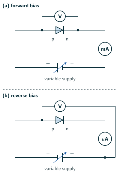
- A diode is forward biased when its p-side is connected to the positive terminal of the battery and its n-side to the negative terminal (NCERT page 334, NCERT Figure 14.13(a)).
- The applied voltage drops mostly across the depletion region, because its resistance, with no free charges in it, is very high compared with the resistance of the p- and n-sides (NCERT page 334). Strictly, it has very few mobile carriers, which the depletion approximation neglects (reasoned).
- NCERT slip (page 334): NCERT calls the depletion region “a region where there are no charges”. It has no free charges, but it does hold charge: the fixed donor and acceptor ions of the space-charge region, as NCERT’s own page 333 and Figure 14.10 show. In an exam, say that the depletion region has no free charge carriers.
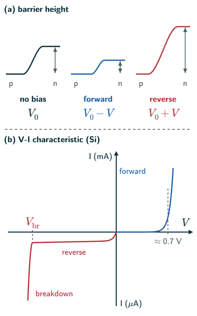
- The applied voltage V is opposite to the built-in potential V0. So the depletion layer becomes thinner and the barrier is lowered (NCERT pages 334–335, NCERT Figure 14.13(b)):
Barrier height in forward bias (NCERT page 335)
- For a small V the barrier falls only slightly, and only the few carriers in the uppermost energy levels can cross: the current is small. A larger V lowers the barrier further, more carriers can cross, and the current increases (NCERT page 335).
- Electrons from the n-side cross the depletion region into the p-side, where they are minority carriers, and holes cross from the p-side into the n-side. NCERT names this process (page 335):
This process under forward bias is known as minority carrier injection.
NCERT Physics Part II (Class 12), Section 14.6.1, page 335
- Near the junction, on each side, the minority carrier concentration rises well above its value far from the junction. The injected carriers therefore diffuse away from the junction edge, giving the current (NCERT page 335, NCERT Figure 14.14).
- The total forward current is the sum of the hole diffusion current and the conventional current due to electron diffusion. It is usually of the order of mA (NCERT page 335).
p-n junction diode under reverse bias
- A diode is reverse biased when its n-side is positive and its p-side negative (NCERT page 335, NCERT Figure 14.15(a)).
- The applied voltage, again mostly across the depletion region, is in the same direction as the barrier potential. The barrier rises and the depletion region widens (NCERT page 335, NCERT Figure 14.15(b)):
Barrier height in reverse bias (NCERT page 335)
- The higher barrier suppresses the flow of electrons from n to p and of holes from p to n, so the diffusion current falls enormously (NCERT page 335).
- The junction field sweeps any electron on the p-side or hole on the n-side that wanders near the junction across to its majority side. This drift current is of the order of a few μA, small because it is carried by minority carriers. It also flows in forward bias, but there it is negligible beside the mA current of the injected carriers (NCERT page 335).
- The reverse current hardly depends on the applied voltage: even a small voltage sweeps the minority carriers across. It is limited by the number of minority carriers on either side, not by the voltage (NCERT pages 335–336).
NCERT gives the forward current as usually in mA and the reverse current as a few μA (page 335). Strictly, actual currents, forward drops and leakage depend on the device, its temperature and the circuit, so a series resistor or a current-limited supply must set the forward current; and V0 − V describes the barrier only while V is below V0 (reasoned).
Circuit for the V-I characteristics
- The V-I characteristic of a diode is the variation of its current with the applied voltage (NCERT page 336).
- The battery is connected to the diode through a potentiometer or rheostat, so that the voltage across the diode can be changed; the current is noted for different voltages and a graph of I against V is drawn (NCERT page 336, NCERT Figure 14.16(a)–(c)).
- The current is measured with a milliammeter in forward bias, where it is large, and with a microammeter in reverse bias (NCERT page 336). The voltage and current are read as in the voltmeter-ammeter circuit for a resistor, but the graph is not a straight line: a diode is not ohmic.
- NCERT slip (page 336): the text says a “micrometer” is used in reverse bias. The instrument is a microammeter, as NCERT Figure 14.16(b) labels it; a micrometer measures length.
- Where the voltmeter goes (beyond the NCERT text): NCERT Figure 14.16(b) puts the voltmeter across the diode alone, so the microammeter also reads the voltmeter’s current, which can match the diode’s μA. In reverse bias, a suitable alternative is to connect the voltmeter across the diode and microammeter together. This avoids voltmeter current in the ammeter but includes the meter’s burden voltage; subtract that drop, or ensure it is negligible.
Threshold voltage and breakdown voltage
- In forward bias the current at first rises very slowly, almost negligibly. Once the voltage across the diode passes a certain value it rises steeply, exponentially, even for a very small rise in voltage. This voltage is called the threshold voltage or cut-in voltage: about 0.2 V for germanium and 0.7 V for silicon (NCERT page 337, NCERT Figure 14.16(c)). Strictly, it marks the approximate bend of the curve on the plotted scale, not a sharp switch (reasoned).
- In reverse bias the current is very small, about a μA, and almost constant as the bias changes: the reverse saturation current (NCERT page 337).
- It stays essentially independent of voltage up to a critical reverse voltage, the breakdown voltage Vbr. There the reverse current rises sharply: a slight increase in voltage causes a large change in current (NCERT page 336).
- If the external circuit does not keep the reverse current below its rated value, set by the manufacturer, the diode is destroyed by overheating. The same happens in forward bias if the forward current exceeds its rated value (NCERT page 336).
- General-purpose diodes are not used beyond the reverse saturation region (NCERT page 337).
- NCERT slip (page 337): NCERT says this action at breakdown “is discussed later in Section 14.8”. The chapter in this reprint ends with Section 14.7; it has no Section 14.8.
- So a diode passes current essentially in one direction, the forward one: its forward resistance is low and its reverse resistance high. This is what makes it a rectifier of ac voltages (NCERT page 337).
- In circuit problems a diode is often taken as ideal: a closed switch, with no voltage drop, in forward bias and an open switch, with no current, in reverse bias. A closer model keeps a fixed drop of about 0.7 V across a conducting silicon diode, as in Example 5 (beyond the NCERT text).
- NCERT slip (page 341): Summary point 13 says the current “is very small (μA) in a p-n junction diode”, leaving out the words in reverse bias. In forward bias it is of the order of mA.
Dynamic resistance
- Because the V-I curve is not a straight line, a diode’s resistance is defined for small changes: the dynamic resistance is the ratio of a small change in voltage ΔV to the small change in current ΔI it causes (NCERT Eq. (14.6), page 337):
Dynamic resistance (NCERT Eq. 14.6)
- It is the inverse of the slope of the V-I curve at that point. Beyond the threshold the curve is steep, so rd is small; in reverse bias the current hardly changes, so the reverse resistance is very large (reasoned from NCERT page 337).
- NCERT slip (page 337): NCERT Example 14.4 treats the curve between 10 mA and 20 mA as a straight line “passing through the origin” and calls the working Ohm’s law. That line, through (0.7 V, 10 mA) and (0.8 V, 20 mA), meets the axis at 0.6 V, not at the origin; ΔV/ΔI is the dynamic resistance of Eq. (14.6), not V/I. Its answer, 10 Ω, is right (see Example 1).
Solved examples
Example 1: Forward and reverse resistance (NCERT Example 14.4)
From NCERT Figure 14.17, a silicon diode carries 10 mA at 0.7 V and 20 mA at 0.8 V; at −10 V the current is −1 μA. Find its resistance (a) at ID = 15 mA, (b) at VD = −10 V.
Answer: (a) rfb = ΔV/ΔI = 0.1 V/10 mA = 10 Ω. (b) NCERT Example 14.4 reads one reverse point and works V/I: rrb = 10 V/1 μA = 1.0 × 10⁷ Ω (page 337). This is a static resistance; on the nearly flat reverse curve ΔV/ΔI is larger still. Either way, the reverse resistance dwarfs the forward one.
Example 2: Forward bias (NCERT Exercise 14.5)
When a forward bias is applied to a p-n junction, it (a) raises the potential barrier; (b) reduces the majority carrier current to zero; (c) lowers the potential barrier; (d) none of the above.
Answer: (c). The barrier falls to V0 − V, and the majority carriers that cross it give a large current (NCERT page 335; NCERT Exercise 14.5, page 342; answer on page 352).
Example 3: Barrier heights
A junction has a built-in potential of 0.7 V. Find the barrier height with a forward bias of 0.5 V and with a reverse bias of 5 V.
Answer: Forward: V0 − V = 0.7 − 0.5 = 0.2 V. Reverse: V0 + V = 0.7 + 5 = 5.7 V (NCERT page 335).
Example 4: Static and dynamic resistance
For the diode of Example 1 at 0.8 V and 20 mA, compare V/I with the dynamic resistance between 10 mA and 20 mA.
Answer: V/I = 0.8/0.020 = 40 Ω, but rd = 0.1/0.010 = 10 Ω. For a non-ohmic device the two differ; NCERT’s Eq. (14.6) defines the dynamic one (beyond the NCERT text).
Example 5: A series resistor
A silicon diode, taken to drop 0.7 V when conducting, is forward biased by a 5 V battery through a resistor. What resistor keeps the current at 20 mA?
Answer: The resistor takes 5 − 0.7 = 4.3 V, so R = 4.3/0.020 = 215 Ω (threshold from NCERT page 337; the rest beyond the NCERT text).
Common mistakes to avoid
Common mistake
Connecting the p-side to the negative terminal for forward bias
Forward bias means p to positive and n to negative; the reverse connection is reverse bias (NCERT pages 334–335).
Common mistake
Taking the reverse current to be exactly zero
A small reverse current of minority carriers, of the order of μA, flows; it is nearly independent of the voltage (NCERT pages 335–337).
Common mistake
Using V/I as the dynamic resistance
Dynamic resistance is ΔV/ΔI, the inverse slope of the V-I curve at the operating point (NCERT Eq. (14.6), page 337).
Quick revision summary
- Forward bias (p to +): barrier V0 − V, minority carrier injection, current in mA once past the threshold voltage, about 0.7 V for Si and 0.2 V for Ge.
- Reverse bias (n to +): barrier V0 + V, wider depletion region, a tiny drift current of minority carriers in μA, nearly constant until the breakdown voltage.
- The V-I curve is taken with a variable supply, a voltmeter across the diode, and a milliammeter (forward) or microammeter (reverse) in series.
- Dynamic resistance rd = ΔV/ΔI: small in forward bias, very large in the nearly flat reverse-saturation region, but small again in breakdown.
Formula sheet
- Forward barrier = V0 − V
- Reverse barrier = V0 + V
- rd = ΔV/ΔI
Questions students ask
What is the difference between forward bias and reverse bias?
In forward bias a diode’s p-side goes to the positive terminal and its n-side to the negative, so the barrier falls to V0 − V and majority carriers cross it in large numbers, giving a current of mA; in reverse bias the connections are swapped, the barrier rises to V0 + V and only a drift of minority carriers, a few μA, is left (NCERT pages 334–335). So the forward resistance is low and the reverse resistance very high (NCERT page 337): past the threshold the forward current rises steeply, while the reverse current stays almost constant up to breakdown (NCERT pages 336–337).
Are knee voltage, cut-in voltage and barrier potential the same?
Knee voltage and cut-in voltage are the same, NCERT’s threshold voltage, where a diode’s forward current starts to rise steeply, about 0.7 V for silicon and 0.2 V for germanium (NCERT page 337); the barrier potential V0 is different: the built-in potential difference of an unbiased junction (NCERT page 335). They are similar in size because a large current flows only once the bias has cut the barrier, V0 − V, to a small value (reasoned). Beyond the NCERT text, the knee is not a sharp point: the current grows exponentially throughout, and the knee is just where this shows on a mA scale (Wikipedia, “Diode”).
What is the diode equation for the V-I characteristic of a p-n junction diode?
In its diffusion-dominated, low-injection regime before breakdown and significant series-resistance effects, a p-n diode approximately follows the ideal Shockley equation, I = I0[exp(eV/kT) − 1], beyond the NCERT text, where I0 is the reverse saturation current and kT/e is about 26 mV at 300 K (Wikipedia, “Shockley diode equation”). In forward bias the −1 soon becomes negligible and the current grows about tenfold for every 60 mV, the steep rise NCERT calls exponential; beyond about 0.15 V of reverse bias the exponential term is under 0.01, so I ≈ −I0, the nearly constant reverse saturation current (NCERT page 337). Real diodes often require an ideality factor η, replacing kT by ηkT; the voltage per current decade is then about 60η mV at 300 K. Recombination, series resistance and breakdown limit this model (Wikipedia, “Shockley diode equation”).
Practice questions
Try each question first, then open the answer to check your working.
-
Q1. Why does the applied voltage drop mostly across the depletion region of a diode?
Show answerHide answer
The depletion region has no free charges, so its resistance is very high compared with that of the p- and n-sides (NCERT page 334). Strictly, it has very few mobile carriers, which the depletion approximation neglects (reasoned).
-
Q2. What limits the reverse current of a diode below breakdown?
Show answerHide answer
The number of minority carriers on either side of the junction, not the applied voltage; even a small voltage sweeps them across (NCERT pages 335–336).
-
Q3. Between 0.75 V and 0.80 V a diode’s current rises from 15 mA to 25 mA. Find its dynamic resistance there.
Show answerHide answer
rd = ΔV/ΔI = 0.05 V/10 mA = 5 Ω (NCERT Eq. (14.6), page 337).