Intrinsic semiconductor
NCERT Class 12 Physics Chapter 14 Section 14.3
Quick answer
An intrinsic semiconductor is an undoped semiconductor whose thermal-equilibrium electron and hole densities satisfy ne = nh = ni. In Si and Ge, the bond picture describes thermal generation of electron-hole pairs, and their drift currents add as I = Ie + Ih. The ideal equilibrium crystal has no thermal carriers at 0 K; illumination can raise carrier densities above ni.
With your textbook
NCERT Physics Part II (Class 12), Chapter 14 “Semiconductor Electronics: Materials, Devices and Simple Circuits”, Section 14.3 “Intrinsic Semiconductor”, pages 327–329.
Open the official NCERT chapter (PDF, 1.9 MB, ncert.nic.in) (opens in a new tab)
Checked against the 2025-26 reprint on .
What is an intrinsic semiconductor?
Intrinsic semiconductor
An intrinsic semiconductor is a pure semiconductor such as silicon or germanium. Its charge carriers are made in the crystal itself, mainly by thermal energy, which breaks a few covalent bonds: each break frees an electron and leaves behind a vacancy with an effective positive charge. In NCERT’s words:
This vacancy with the effective positive electronic charge is called a hole.
NCERT Physics Part II (Class 12), Section 14.3, page 327
In thermal equilibrium, an ideal undoped semiconductor has equal numbers of free electrons and holes, ne = nh = ni, the intrinsic carrier concentration (NCERT Eq. (14.1), page 327).
In plain words: every silicon atom holds hands with four neighbours through shared electrons. Heat shakes a few of these bonds loose. The electron that escapes can wander and carry current, and the empty place it leaves behind also seems to wander, as neighbouring electrons hop into it one after another, like a gap moving along a queue.
The bond picture is an introductory model of band excitations. Illumination or carrier injection can raise both densities above ni; ni denotes the thermal-equilibrium value, not every illuminated state. Numerical values below use NCERT’s stated room-temperature approximation.
Electrons and holes
- Ge and Si have a diamond-like crystal structure: each atom is surrounded by four nearest neighbours (NCERT page 327; NCERT Figure 14.3 gives the lattice spacing a as 3.56, 5.43 and 5.66 Å for carbon, silicon and germanium).
- Si and Ge have four valence electrons. Each atom shares one of its four valence electrons with each of its four neighbours, and takes a share of one electron from each. These shared pairs form covalent (valence) bonds (NCERT page 327).
- At ideal 0 K there are no thermally generated carriers; at low but finite temperature their population is very small (NCERT page 327, NCERT Figure 14.4).
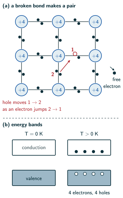
- As the temperature rises, thermal energy breaks a few bonds. The freed electron, charge −q, becomes a conduction electron, and the bond it left has a vacancy with an effective charge +q: a hole, which behaves as an apparent free particle with positive charge (NCERT page 327, NCERT Figure 14.5(a)).
- In an intrinsic semiconductor in thermal equilibrium the free-electron and hole densities each equal ni (NCERT Eq. (14.1), page 327):
Intrinsic carrier concentration (NCERT Eq. 14.1)
- How a hole moves. An electron from a covalent bond at a neighbouring site 2 may jump into the hole at site 1. The hole is now at site 2: it has apparently moved from site 1 to site 2. The electron freed in the first place takes no part in this particular hole-hopping step, although a conduction electron can later recombine with a hole (NCERT page 328, NCERT Figure 14.5(b)).
- Under an electric field the free electrons give an electron current Ie, and the holes, moving towards the negative potential, give a hole current Ih. The motion of holes is just a convenient way of describing the motion of bound electrons into empty bonds (NCERT page 328). The total current is (NCERT Eq. (14.2), page 328):
Total current (NCERT Eq. 14.2)
Thermal generation of carriers
- Alongside the generation of electron-hole pairs there is recombination, when an electron collides with a hole and fills it. At equilibrium the rate of generation equals the rate of recombination (NCERT page 328).
- At T = 0 K an intrinsic semiconductor behaves like an insulator: the valence band is full and the conduction band empty. At T > 0 K thermal energy lifts some electrons from the valence band into the conduction band, leaving an equal number of holes in the valence band (NCERT page 329, NCERT Figure 14.6).
- The conductivity of an intrinsic semiconductor depends on its temperature, but at room temperature it is very low, low compared with doped material. Doping controls the carrier type and concentration for junction devices; intrinsic regions are nevertheless useful in detectors and p-i-n devices. Semiconductors are therefore often doped (NCERT page 329).
- For silicon, ni ≈ 1.5 × 10¹⁶ m−3, against about 5 × 1028 atoms m−3 (NCERT Example 14.2, page 332): the carrier-to-atom density ratio is about one to 3.3 × 10¹². This is a population comparison, not a count of permanently ionised atoms (see Example 1).
- As the temperature rises, more bonds break and ni grows, so the resistivity of a pure semiconductor falls with temperature, unlike a metal’s, which rises (NCERT Chapter 3, pages 90–91).
- Low-field drift conductivity (beyond the NCERT text): with mobilities μe and μh (drift speed per unit field), σ = e(neμe + nhμh), which for an intrinsic semiconductor is eni(μe + μh).
Conductivity (beyond the NCERT text)
- In silicon and germanium electrons are more mobile than holes, so in a homogeneous pure sample under the same weak field the electron current is larger even though ne = nh (beyond the NCERT text).
Solved examples
Example 1: How few carriers?
Pure silicon has about 5 × 1028 atoms m−3 and ni = 1.5 × 10¹⁶ m−3. What is the ratio of the free-electron density to the atomic density?
Answer: (1.5 × 10¹⁶)/(5 × 1028) = 3 × 10⁻¹³, about one conduction electron per 3.3 × 10¹² atoms (data from NCERT Example 14.2, page 332).
Example 2: Electrons and holes in pure silicon
Using NCERT’s room-temperature value ni = 1.5 × 10¹⁶ m−3, how many free electrons and holes are there per cubic metre of pure silicon in equilibrium?
Answer: In an intrinsic semiconductor ne = nh = ni, so 1.5 × 10¹⁶ m−3 of each (NCERT Eq. (14.1), page 327; ni from NCERT Example 14.2, page 332).
Example 3: Conductivity of pure silicon
Taking μe = 0.135 m2 V−1 s−1 and μh = 0.048 m2 V−1 s−1, find the conductivity and resistivity of pure silicon with ni = 1.5 × 10¹⁶ m−3.
Answer: σ = eni(μe + μh) = 1.6 × 10−19 × 1.5 × 1016 × 0.183 ≈ 4.4 × 10⁻⁴ S m−1, so ρ = 1/σ ≈ 2.3 × 10³ Ω m, inside the semiconductor range of NCERT page 324 (beyond the NCERT text).
Example 4: Which way do holes drift?
A field is applied across a pure germanium crystal. Which way do the electrons and holes drift, and how do their currents add?
Answer: Electrons drift towards the positive end and holes towards the negative end. Both motions carry current in the direction of the field, so the currents add: I = Ie + Ih (NCERT page 328).
Common mistakes to avoid
Common mistake
Thinking the hole current is the free electrons moving backwards
The hole moves because bound electrons hop from bond to bond into the vacancy; the free conduction electrons are a separate current (NCERT page 328).
Common mistake
Expecting more electrons than holes in a pure semiconductor
Thermal pair generation gives one electron and one hole; in the equilibrium intrinsic model ne = nh = ni (NCERT Eq. (14.1), page 327).
Common mistake
Thinking an intrinsic semiconductor conducts at absolute zero
At 0 K no bonds are broken, so there are no carriers and it behaves like an insulator (NCERT page 329).
Quick revision summary
- In Si and Ge each atom forms four covalent bonds with its neighbours.
- Heat breaks a few bonds: a free electron and a hole, an effective positive charge, are made in pairs.
- In thermal equilibrium, ne = nh = ni; the current is I = Ie + Ih.
- Generation and recombination balance at equilibrium; at 0 K the crystal is an insulator.
- NCERT’s room-temperature value for silicon is ni ≈ 1.5 × 10¹⁶ m−3, so pure silicon conducts poorly; σ = e(neμe + nhμh) (beyond the NCERT text).
Formula sheet
- ne = nh = ni
- I = Ie + Ih
- σ = e(ne μe + nh μh)
Questions students ask
What is the difference between intrinsic and extrinsic semiconductors?
An intrinsic semiconductor is an undoped semiconductor (such as Si or Ge) in which thermal-equilibrium free-electron and hole densities are equal, ne = nh = ni, while an extrinsic semiconductor is doped with a few parts per million of a pentavalent or trivalent impurity, so that one kind of carrier far outnumbers the other and the conductivity is many times higher (NCERT pages 327–331). Intentional dopants add donor or acceptor levels close to the band edges. Defects and surfaces can also introduce gap states; purity alone does not exclude every such state.
Do holes have mass, and why are electrons more mobile than holes?
A hole is a quasiparticle describing a missing valence-band electron. Its effective mass describes how that excitation responds to a force; it is not the bare mass of a new elementary particle. In silicon, electron mobility is higher than hole mobility. Mobility depends on both band effective mass and scattering time, roughly μ = eτ/m*, so mass alone does not determine it. The example values here give μe/μh ≈ 2.8 (see BYU semiconductor constants for representative values).
Why is silicon preferred to germanium in semiconductor devices?
Silicon is preferred to germanium because its band gap is larger, 1.1 eV against 0.7 eV (NCERT page 332), so heat breaks far fewer bonds: germanium’s intrinsic carrier concentration at room temperature, about 2 × 10 m, is over a thousand times NCERT’s 1.5 × 10 m for silicon (NCERT Example 14.2, page 332; germanium beyond the NCERT text, Ioffe Institute data). So silicon diodes have a smaller reverse current and work at higher temperatures (reasoned). Beyond the NCERT text, silicon is also the second most abundant element in Earth’s crust and easily grows an insulating oxide film (Wikipedia, “Silicon”).
What is the formula for intrinsic carrier concentration, and how does it change with temperature?
The intrinsic carrier concentration follows ni ∝ T3/2 exp(−Eg/2kT), beyond the NCERT text, with k Boltzmann’s constant, assuming nondegenerate parabolic bands and approximately fixed effective masses; Eg can itself vary with temperature (MIT, law of mass action); NCERT defines ni only as the equal number of free electrons and holes per unit volume, ne = nh = ni (NCERT Eq. (14.1), page 327). So ni rises very steeply: for silicon, with Eg ≈ 1.1 eV, each 10 K rise near room temperature roughly doubles it (reasoned). That is why a pure semiconductor’s resistivity falls so fast on heating.
What happens when an electron and a hole recombine?
When an electron recombines with a hole, it drops from the conduction band into the empty bond in the valence band, and both carriers disappear (NCERT page 328). Beyond the NCERT text, the electron gives up an energy of about Eg: in silicon and germanium it goes mostly into lattice vibrations, as heat, because their band gaps are indirect, while direct-gap compounds such as gallium arsenide allow efficient radiative recombination in suitably designed light-emitting devices. Non-radiative channels still exist; not every recombination emits a photon (Wikipedia, “Direct and indirect band gaps” and “Band gap”).
Practice questions
Try each question first, then open the answer to check your working.
-
Q1. What is a hole, and what charge does it carry?
Show answerHide answer
A vacancy in a covalent bond left when an electron breaks free; it behaves like a free particle with an effective positive charge +q (NCERT page 327).
-
Q2. Why does pure silicon behave like an insulator at 0 K?
Show answerHide answer
At 0 K no thermal energy breaks the bonds: the valence band is full and the conduction band empty, so there are no free electrons or holes (NCERT page 329).
-
Q3. Why is the resistivity of pure germanium lower at 60 °C than at 20 °C?
Show answerHide answer
More thermal energy breaks more bonds, so there are more electrons and holes to carry current (reasoned from NCERT pages 327–329).